Robust I2C slave without a sampling clock
25 Aug 2011
Updated 2 May 2020
I2C is a popular two-wire serial bus protocol for communicating between devices. Most MCUs support it, so it’s a good choice of interface for many chips. This article shows how to implement an I2C slave interface without the use of a bus sampling clock.
Bus sampling is a simple way to implement an I2C slave, but in order to support reasonable I2C transfer rates, you need a sampling clock frequency of several MHz. This is fine if the rest of your device already needs such a fast clock, but if it doesn’t, then power consumption is needlessly increased. A robust I2C slave can be implemented using nothing but the bus signals for clocking. This has the advantage that the slave interface consumes no power (save for leakage currents) when the bus is idle.
The scheme described here can support any bus speed and is highly reliable. It’s compatible with multi-master buses, and doesn’t require the master support delayed acknowledgement or clock-stretching.
Overview of the I2C protocol
The I2C bus consists of two lines: SCL (serial clock)
and SDA (serial data), both of which are normally held at
logic high via a weak pull-up resistor. Devices control the bus by
choosing to pull lines to logic low, or leaving their outputs
high-impedance. This is the basic mechanism behind multi-master
arbitration, but this won’t be covered here – for simplicity, we’ll
assume a single master with multiple slaves.
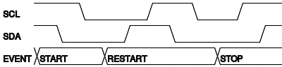
There are three special events generated by the master, called
START, STOP and RESTART. These
are used, respectively, to being a transaction, end a transaction, and
start a new transaction without releasing control of the bus. Timing
diagrams for these three events are shown here:
There are two types of byte transfer events: master-to-slave and slave-to-master. The timing for both is the same:

Data bits are placed on SDA MSB-first. In a
master-to-slave transaction, the master clocks out a data byte over the
first 8 cycles, and then the slave acknowledges on the 9th cycle by
pulling SDA low. A slave-to-master transaction is exactly
the reverse, except that the master only acknowledges if it wishes the
slave to transmit another byte. Without this rule, the slave might
continue to pull SDA down for the next cycle, preventing
the master from being able to generate a RESTART or a
STOP event.
The master controls SCL (except in the case of clock
stretching, which isn’t covered here). SDA may only change
while SCL is low, except when the master is generating a
START/RESTART/STOP event.
Transaction structure
All transactions begin, after a START or
RESTART event, with a master-to-slave transfer containing
an address byte. The upper 7 bits of the address byte are the slave
address, and the LSB is the R/W# bit, which signifies the
direction of the following transfers (low for master-to-slave, high for
slave-to-master). If the slave address is recognised by a device on the
bus, it acknowledges on the 9th SCL pulse by pulling
SDA low. Other devices must ignore the remainder of the
transaction. The transaction ends with a RESTART or
STOP event.
Typical use
Most slave devices have a number of indexed internal registers. The way I2C is usually used to manipulate the internal registers of such devices is described here. To write a register, the master initiates a write transaction to the desired device. The register index is transferred following the device address, and then the desired data. For example, to write 0x57 to register 3 of device 1010101x, the following sequence of events occurs:
STARTMaster-to-slave: device address,
R/W#= 0 (0xAA)Master-to-slave: register index (0x03)
Master-to-slave: register data (0x57)
STOP
Read transactions are slightly more complex. Since I2C transactions
are unidirectional, two transactions are needed, divided by a
RESTART. The first (write transaction) sends the register
index to the device, and the value is sent in the next transaction
(read). For example, to read back the value written in the previous
example, the following sequence of bus events occurs:
STARTMaster-to-slave: device address,
R/W#= 0 (0xAA)Master-to-slave: register index (0x03)
RESTARTMaster-to-slave: device address,
R/W#= 1 (0xAB)Slave-to-master (not acked): register data (0x57)
STOP
Two conventions are usually adopted to make this system more convenient:
The internal register index is incremented after each transfer. This allows efficient bulk transfer of a block of data to/from logically contiguous registers.
The internal register index is reset to 0 following a
STARTevent (but notRESTART). Typically, register 0 is a status register, so this allows efficient polling of the status register with a single I2C transaction.
The implementation described in this article follows this conventional scheme.
Implementation
For this implementation, we will assume an asynchronous reset input,
though this won’t be shown in circuit diagrams. There is an
SCL input, and a tri-state SDA port. Other
interfaces are not covered explicitly.
The flip-flops will be driven mostly by SCL. Input data
latching must be done on the rising edge, as this is the only time we
can guarantee stable data. Conversely, output latching must be done on
the falling edge of SCL. Internal logic may operate on any
edge, but here we use the falling edge consistently.
START/STOP/RESTART
First, we need to be able to detect a START event. The
following pair of flip-flops will do that:
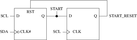
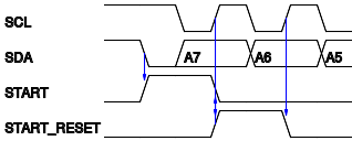
This generates a pulse lasting from the START event
itself to the next rise of SCL (covering exactly one
falling edge) as shown in the timing diagram:
The Verilog implementation of this is:
reg             start_detect;
reg             start_resetter;
wire            start_rst = RST | start_resetter;

always @ (posedge start_rst or negedge SDA)
begin
        if (start_rst)
                start_detect <= 1'b0;
        else
                start_detect <= SCL;
end

always @ (posedge RST or posedge SCL)
begin
        if (RST)
                start_resetter <= 1'b0;
        else
                start_resetter <= start_detect;
end
The STOP detector is similar, except for the sense of
the SDA clock input:
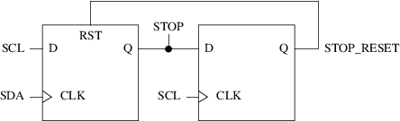
It generates a pulse from the STOP event to the next
rise of SCL, again covering exactly one fall of SCL in the
next transaction:
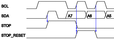
The Verilog implementation is:
reg             stop_detect;
reg             stop_resetter;
wire            stop_rst = RST | stop_resetter;

always @ (posedge stop_rst or posedge SDA)
begin
        if (stop_rst)
                stop_detect <= 1'b0;
        else
                stop_detect <= SCL;
end

always @ (posedge RST or posedge SCL)
begin
        if (RST)
                stop_resetter <= 1'b0;
        else
                stop_resetter <= stop_detect;
end
Given these two detectors, we don’t need to implement a
RESTART detector – we can distinguish between a
START and a RESTART by checking to see if a
STOP event has occured prior to the
START/RESTART. Of course, the first
START after reset will be misinterpreted as a
RESTART, but in practice this doesn’t matter, since we will
reset the index pointer on reset anyway.
Latching input data
To keep track of what stage a transfer is in, we need a modulo-9
counter. It needs to be triggered on the falling edge of SCL, so that it
can reset with START events:
reg [3:0]       bit_counter;

wire            lsb_bit = (bit_counter == 4'h7) && !start_detect;
wire            ack_bit = (bit_counter == 4'h8) && !start_detect;

always @ (negedge SCL)
begin
        if (ack_bit || start_detect)
                bit_counter <= 4'h0;
        else
                bit_counter <= bit_counter + 4'h1;
end
We need to latch data bits into a shift register as they appear:
reg [7:0]       input_shift;

parameter [6:0] device_address = 7'h55;
wire            address_detect = (input_shift[7:1] == device_address);
wire            read_write_bit = input_shift[0];

always @ (posedge SCL)
        if (!ack_bit)
                input_shift <= {input_shift[6:0], SDA};
Not shifting on the ACK bit means that the data is complete and
stable for two clock cycles, which is useful later. Note that since the
data is shifted on the positive edge of SCL, we have a
complete data byte for two falling edges of SCL – once with
lsb_bit high, and once with ack_bit high. We
need a separate means of detecting acknowledgement during a
slave-to-master transfer:
reg             master_ack;

always @ (posedge SCL)
        if (ack_bit)
                master_ack <= ~SDA;
State machine
Having constructed input handling logic, we can now use it to control a state machine. This machine’s states remain stable over an entire transfer, changing at the boundary between transfers, or between transfers and special events. The state transition diagram is:
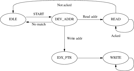
The occurance of a START condition acts as a state
machine synchronous reset:
parameter [2:0] STATE_IDLE      = 3'h0,
                STATE_DEV_ADDR  = 3'h1,
                STATE_READ      = 3'h2,
                STATE_IDX_PTR   = 3'h3,
                STATE_WRITE     = 3'h4;

reg [2:0]       state;
wire            write_strobe = (state == STATE_WRITE) && ack_bit;

always @ (posedge RST or negedge SCL)
begin
        if (RST)
                state <= STATE_IDLE;
        else if (start_detect)
                state <= STATE_DEV_ADDR;
        else if (ack_bit)
        begin
                case (state)
                STATE_IDLE:
                        state <= STATE_IDLE;

                STATE_DEV_ADDR:
                        if (!address_detect)
                                state <= STATE_IDLE;
                        else if (read_write_bit)
                                state <= STATE_READ;
                        else
                                state <= STATE_IDX_PTR;

                STATE_READ:
                        if (master_ack)
                                state <= STATE_READ;
                        else
                                state <= STATE_IDLE;

                STATE_IDX_PTR:
                        state <= STATE_WRITE;

                STATE_WRITE:
                        state <= STATE_WRITE;
                endcase
        end
end
Register transfers
Before handling register transfers, we need to maintain the state of
the index pointer. This index is loaded by the first transfer in a write
transaction, incremented every other transfer, and reset on a
START condition (but not RESTART). It is
implemented as follows:
always @ (posedge RST or negedge SCL)
begin
        if (RST)
                index_pointer <= 8'h00;
        else if (stop_detect)
                index_pointer <= 8'h00;
        else if (ack_bit)
        begin
                if (state == STATE_IDX_PTR)
                        index_pointer <= input_shift;
                else
                        index_pointer <= index_pointer + 8'h01;
        end
end
Handling register writes is straight-forward. For each register, once per transfer, we check to see if it’s being addressed for writing, and if so, we latch the value in the input shift register. For example, to handle writes to a register that has index 0x03:
reg [7:0]       reg_03;

always @ (posedge RST or negedge SCL)
begin
        if (RST)
                reg_03 <= 8'h00;
        else if (write_strobe && (index_pointer == 8'h03))
                reg_03 <= input_shift;
end
To handle read requests, it’s most convenient internally to deal with byte transfers. In order to do this, we need an output shift register. It must be loaded before the ACK bit, in order to be ready for the output stage:
reg [7:0]       output_shift;

always @ (negedge SCL)
begin
        if (lsb_bit)
        begin
                case (index_pointer)
                8'h00: output_shift <= reg_00;
                8'h01: output_shift <= reg_01;
                // ... and so on ...

                endcase
        end
        else
                output_shift <= {output_shift[6:0], 1'b0};
end
Output driver
Finally, we’re ready to implement the output driver. We latch the output driver control signal to prevent bus glitches. The signal switches the driver between two states: high-impedance and pull-low. We pull low only under the following circumstances:
Acknowledging an address.
Acknowledging a master-to-slave transfer.
Transmitting a zero during a slave-to-master transfer.
The logic is a little subtle, because we have to set the state for
the next SCL clock cycle, taking into
account that the state machine’s state for the next cycle may not be the
same as what it is for the current cycle (note in particular the logic
for delivering the first bit of the first transfer in a read
transaction):
reg             output_control;
assign          SDA = output_control ? 1'bz : 1'b0;

always @ (posedge RST or negedge SCL)
begin
        if (RST)
                output_control <= 1'b1;
        else if (start_detect)
                output_control <= 1'b1;
        else if (lsb_bit)
        begin
                output_control <=
                    !(((state == STATE_DEV_ADDR) && address_detect) ||
                      (state == STATE_IDX_PTR) ||
                      (state == STATE_WRITE));
        end
        else if (ack_bit)
        begin
                // Deliver the first bit of the next slave-to-master
                // transfer, if applicable.
                if (((state == STATE_READ) && master_ack) ||
                    ((state == STATE_DEV_ADDR) &&
                        address_detect && read_write_bit))
                        output_control <= output_shift[7];
                else
                        output_control <= 1'b1;
        end
        else if (state == STATE_READ)
                output_control <= output_shift[7];
        else
                output_control <= 1'b1;
end
Synchronization
It’s unlikely that a device will be clocked solely by
SCL. There will probably be other internal clock domains,
and the I2C interface must be able to transfer data to and from these
domains.
A two-phase REQ/ACK scheme is unsuitable in most cases due to the intermittent clock driving the I2C interface. However, since the device is likely being addressed by an MCU, software assistance on the part of the master can make the task easier.
Write synchronization
Provided data is not written more than once every few cycles of the other clock domain, a single-phase synchronization scheme is feasable. For each writable piece of data which must be synchronized, implement a data phase bit. Whenever the register is written, toggle the data phase register.
In the other clock domain, the data phase bit is sampled through a two-flop synchronizer. When a change is detected in the sampled data phase signal, the data in the I2C slave interface register can be latched into a register in the other clock domain.
This general scheme is fairly flexible, but other schemes may be possible, depending on the application. One simple scheme is to designate one bit in an I2C interface register to be an asynchronous reset for logic in the other domain, and require that software only change configuration registers while this reset is asserted.
Read synchronization
Since there is no minimum speed for I2C transfers, a data-phase toggle scheme as described above can’t be guaranteed to work correctly for reads. Instead, negotiation is required between the MCU and the internal logic via the I2C interface.
For example, one control bit in an I2C register may be designated a
“read-request” bit. This could trigger the internal logic to update the
data presented and set a “read-ready” bit. The read-ready bit can be
sampled through a two-flop synchronizer driven by SCL (this
is always possible for single bits). By the time the device has been
addressed, the state of the synchronized read-ready bit should be up to
date. At this point, the MCU can check the sampled bit and then decide
whether it’s possible to read the appropriate data register.
This scheme is a natural fit to reading the results of “one-shot” tasks. In many cases, the MCU will request a task to be executed by means of a control bit. It can then poll a status bit to be notified of task completion (with associated return data).
Caveats
This design uses both edges of SCL and SDA to drive flip-flops. For this to be safe, these lines must be glitch-free and they must adhere to I2C timing requirements.
If you’re taking these lines directly from the outside or via FPGA IO buffers without passing through any combinatorial logic gates, then you may assume you’re not introducing glitches that weren’t already present.
It would be a good idea to expose an asynchronous reset if your design is being driven from an externally-supplied I2C bus.